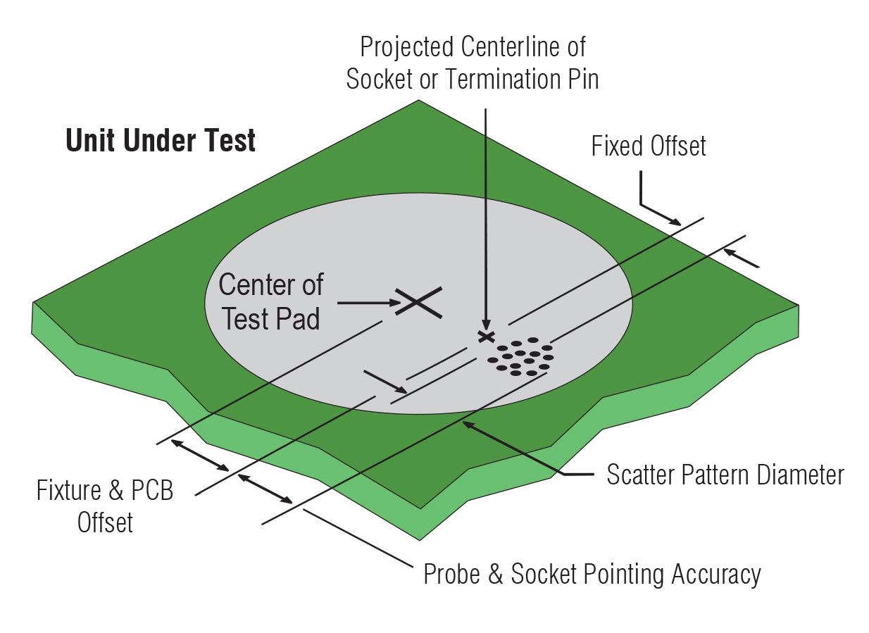
As space on printed circuit boards (PCBs) becomes increasingly limited, reliable contact of smaller test targets becomes a requirement. By improvingmanufacturing and assembly methods and designing for testability, false test failures can be greatly reduced.
During the electrical testing of PCBs, spring test probes contact the test targets on the unit under test (UUT). These targets include but are not limited to pads, vias, leads, posts, components, and connectors. In an ideal situation, the probe tip will contact the test target every time. Unfortunately, the manufacturing tolerance stack-up which includes the board, fixture, and probes may cause the probe to miss the target.
The following information is meant to explain the variables, defines the tests, and most importantly, provides engineers and designers with the needed accuracy specifications for probe products made by QA Technology. This can be used in conjunction with tolerances from the test fixture and PCB to properly size test pads for reliable contact.
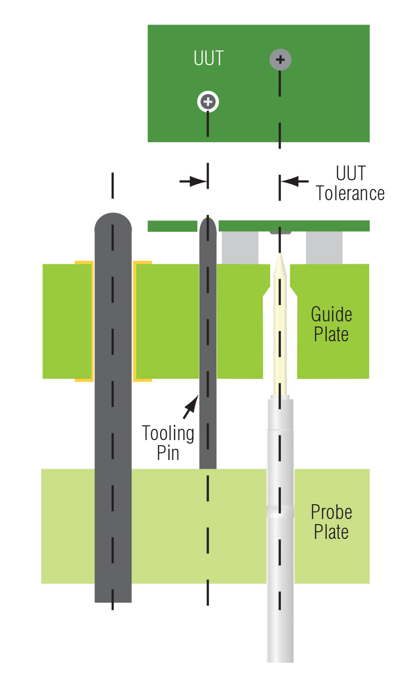
When discussing the ability of a probe to contact its intended target, the effects of standard groups of tolerances must be classified. The tolerances which affect a probe’s ability to contact its target on the UUT can be broadly divided into the following groups:
Fixture and PCB Offset: This group of tolerances is controlled by the fixture builder and by the PCB manufacturer.
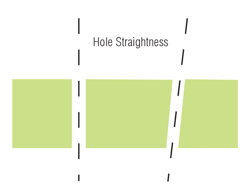
It includes:
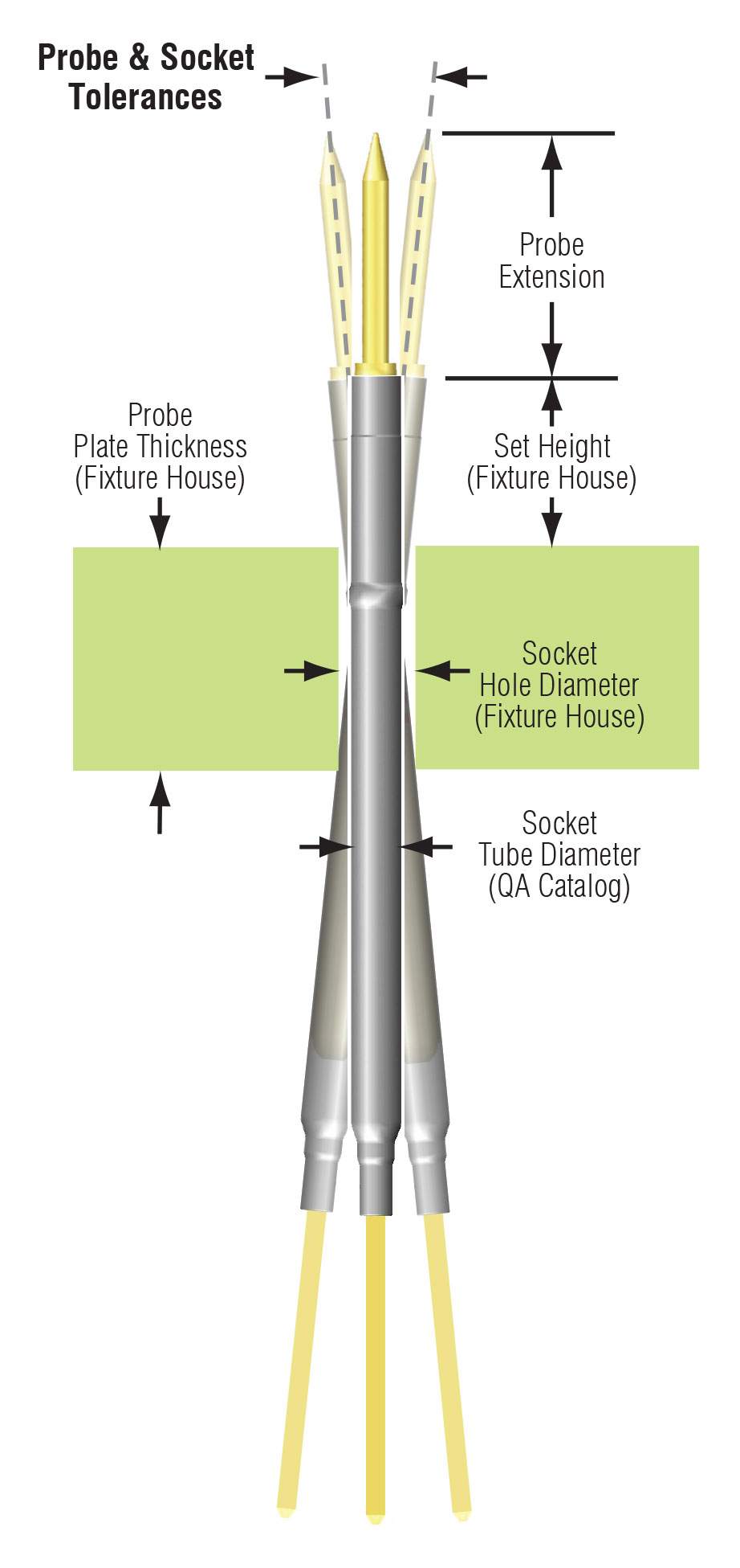
Probe and Socket Tolerances: This is a roughly circular scatter pattern where the probe tip contacts the UUT.
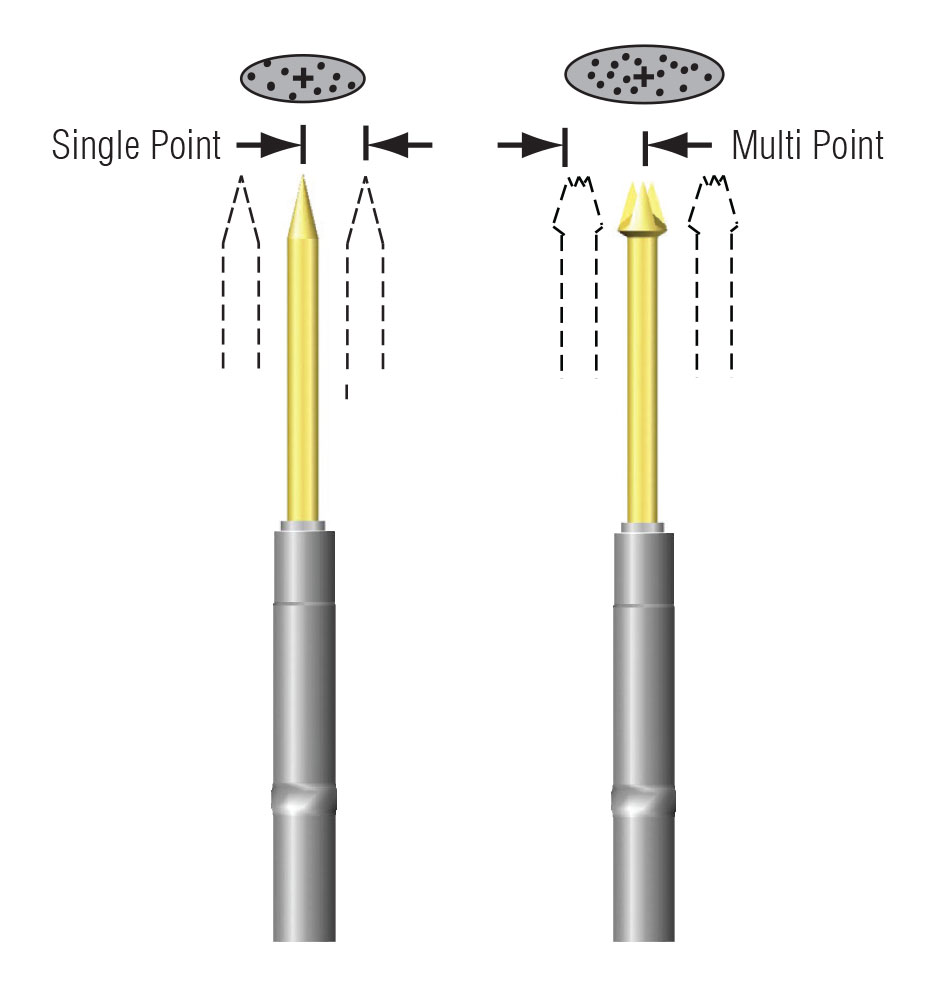
Probe and Socket Pointing Accuracy: The combined effects of the “Fixed Offsets” and one half (½) of the “Scatter Pattern Diameter”. This is measured directly by rotating a probe and socket assembly around the socket’s centerline and measuring the total indicator reading (TIR) at the probes tip. Pointing accuracy = ½ TIR.
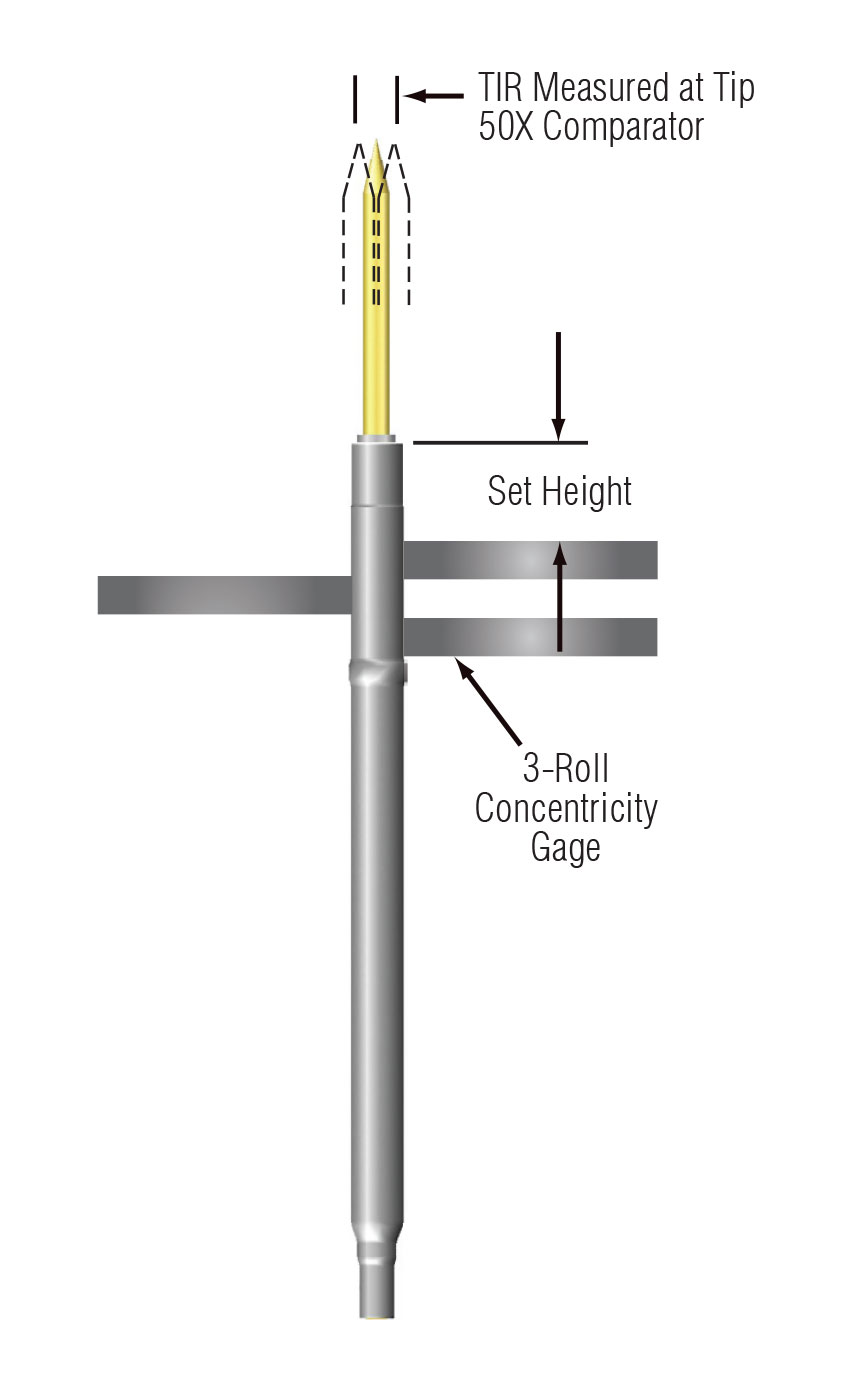
Fifty spear point probes from each series were inserted in their appropriate sockets. Each probe and socket assembly was then mounted in a three-roll concentricity gage at a given set-height, then rotated around its axis to record the TIR.
The set height was determined by the location of the socket’s press ring so that it did not interfere with the rolls on the concentricity gage during the test. The total deviation of the tip was measured with a 50X comparator to calculate the minimum, maximum, average, and standard deviations. Note: The measurements for the X Probe® Series do not include a socket.
The following table summarizes the overall pointing accuracy for each series. The X Probe® series will have better pointing accuracy as it does not utilize a socket. To get a better statistical representation of the data, the standard deviation can be added to the average or mean to show how a population of probes from the same series will respond. These numbers are a more useful average. They give designers a higher confidence level that they will be able to meet design for test (DFT) objectives.
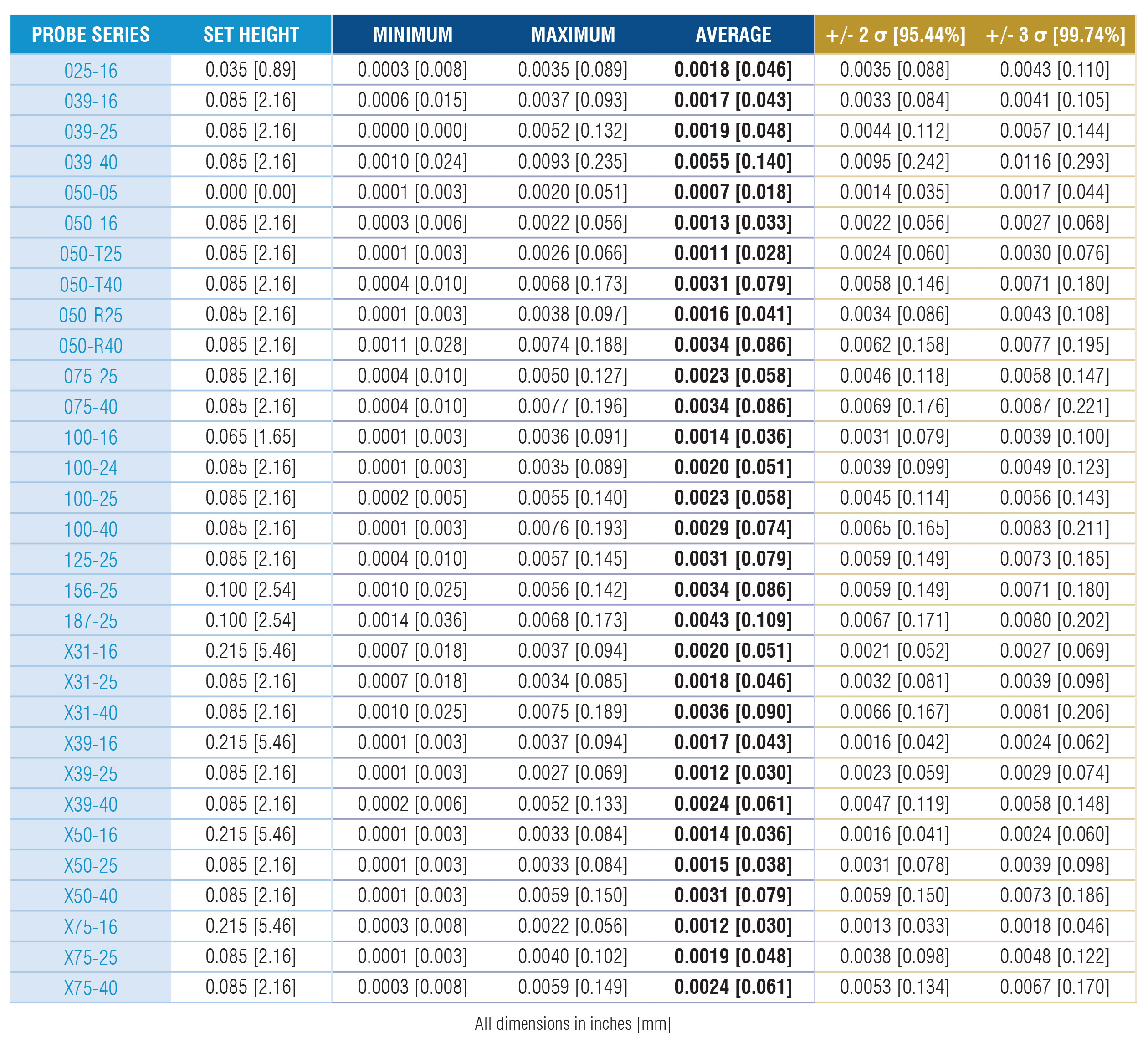
The probe accuracy specifications listed above can be used together with fixture and PCB tolerances to accurately size the smallest test pad necessary for reliable contact.
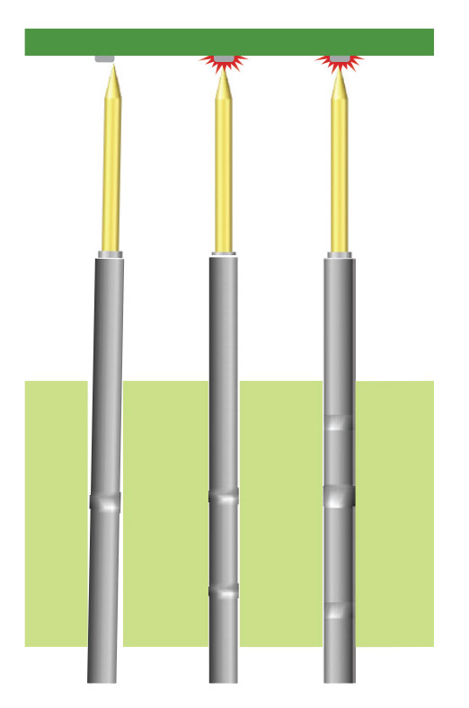
To improve a probe’s TIR in a fixture, use multiple press ring sockets. This feature is offered in our smaller sizes to reduce tilting in the mounting hole. Triple press ring sockets are an exclusive from QA to meet the increased pointing accuracy demands of the ATE industry.
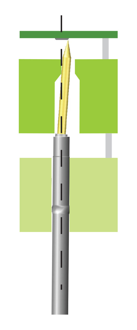
The goal for the end user is a fixture/PCB that delivers high first pass yields. Ensuring that the fixture is aligned, and the sockets and probes are selected and installed properly, will lead to a longer life because of the reduction of sideloading in the finished assembly.
All of the above characteristics of pointing accuracy should be considered when designing and building a fixture to achieve optimal probe performance and cycle life. Otherwise, probe tips may miss the intended target or contact off center causing sideloading which increases probe wear.
Examples that cause extreme sideloading:
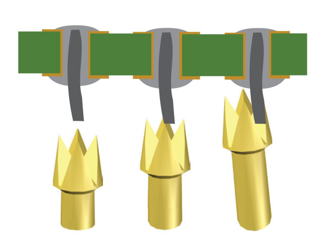
Extreme contact angles create higher internal friction. In the case of a crown point contacting a straight component lead, the lead can fit in the downward sloping valley between the points of the crown and create large sideloads. The plunger will deflect sideways, sometimes to the point where the lead will glance off the side of the head. But before the plunger is pushed sideways enough to break, the test point on the PCB contacts the probe tip and the plunger is compressed. The compressing of the plunger in this state causes an increase in friction between the sliding surfaces of the probe tube and plunger resulting in the increase of wear in the probe assembly. While a probe in this condition may operate as designed for the life of the test fixture, high cycle production test environments may experience shorter probe life requiring an increase in fixture maintenance.
Addressing the factors in the early stages of design will lead to the best possible fixture and probe performance.
The use of Printed Circuit Boards is an important part of our daily lives that is often taken for granted. Designers and manufacturers of PCB’s understand the importance of ensuring that the PCB design, manufacturing, and assembly of these boards meets the highest standards to guarantee a long life and reliable operation. While the factors discussed are only a small part of the overall success of a PCB test system, taking them into consideration and utilizing the design data for the construction of test fixtures will provide long term dividends for our customers. QA’s recommendations for initial board design and for subsequent test procedure will enable appropriate adherence to best practice probe accuracy specifications while increasing cost efficiency, manufacturing quality, performance, accuracy, and testing of PCB products.