Printed Circuit Boards (PCB) are an essential part of the many electronic products we rely on every day. Both in-circuit and functional testing after manufacturing are critical steps to ensuring their dependability. QA Technology’s test probes are an important part of this process, offering the best possible electrical contact with each board being tested.
While there are many probe factors that affect its ability to make reliable electrical contact, proper tip style selection is likely the most important one. Incorrect tip selection could cause false failures where no defects are found (NDF), lower your first pass yields (FPY), or in extreme cases, damage the unit under test (UUT). Selecting the right tip can reduce the overall cost of test by increasing the output of units being tested and extending the life of your test probes.
Test engineers often have very different experiences as to which is the best probe tip style to use for any given contact surface. QA offers a wide range of styles to support the various board test applications known in the industry. The following considerations will help you select the right tip style for many of today’s common test targets.
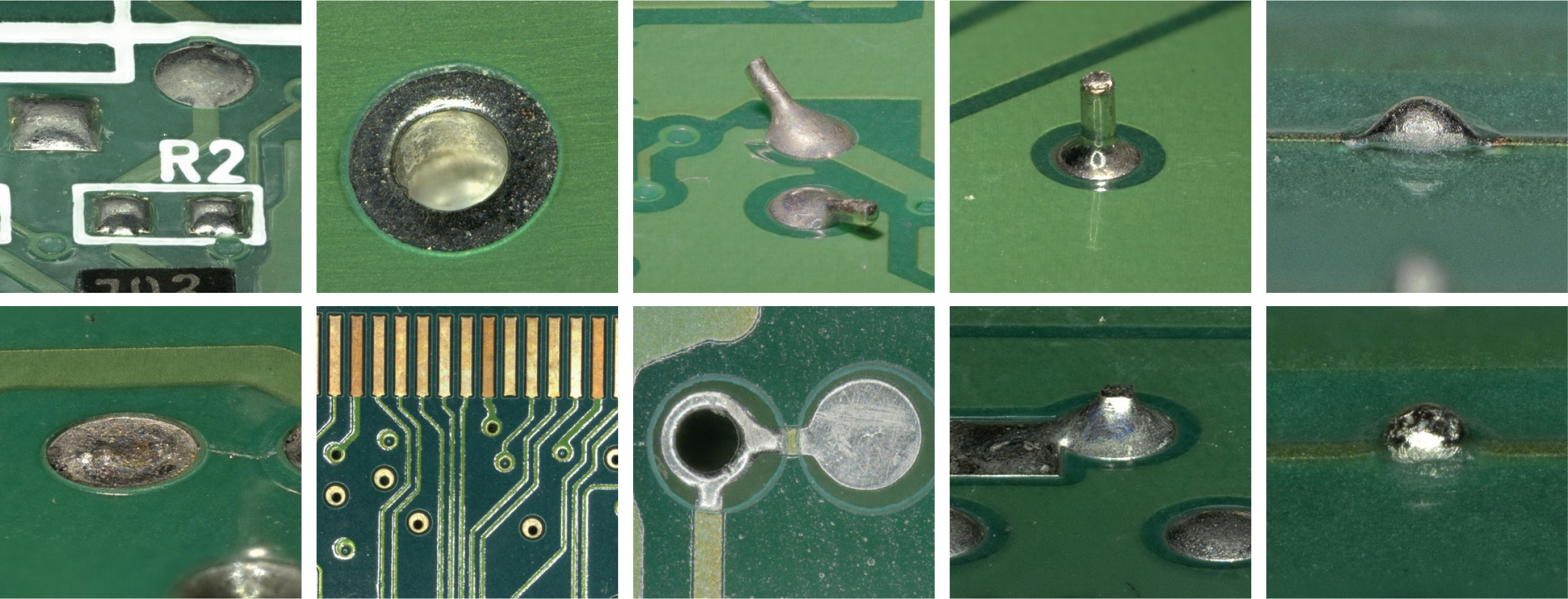
It is important to consider the size, shape and other features of the test targets. There are various PCB targets such as pads, vias, leads, posts, and solder bumps, which range in probe-ability from easy to difficult.
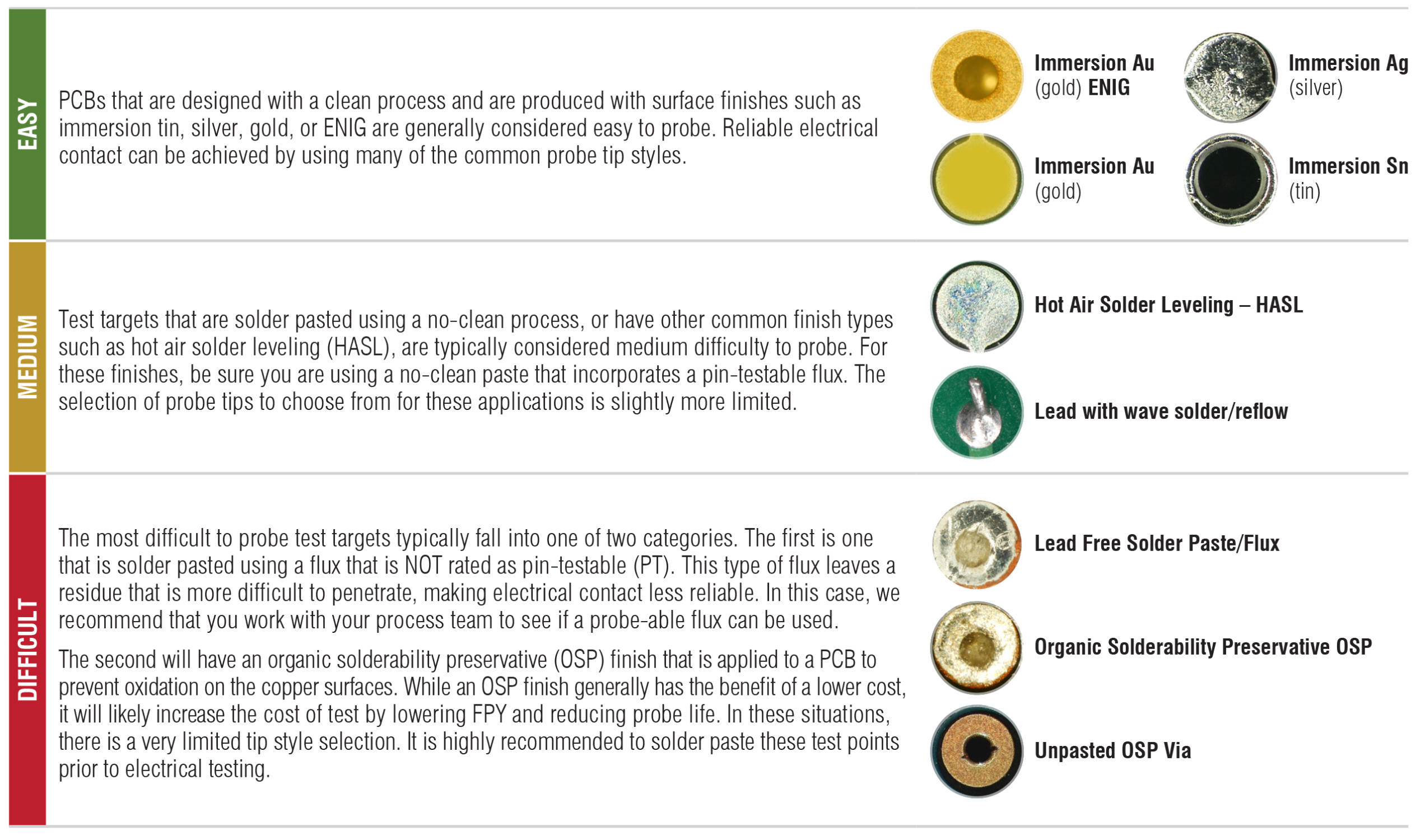
QA’s tips are made from either beryllium copper (BeCu) or steel. Both are gold plated over nickel. The hardness of steel ranges between 58 and 60 on the Rockwell C scale, 38-42 for BeCu. As such, steel will have reduced wear and remain sharp longer.
While there is a difference in the average resistance of less than 10 mOhms between the two base materials, it will not affect the vast majority of test applications.
QA offers many different tip styles, each with their unique geometry. The large number of headed or headless choices supports the wide variety of test applications
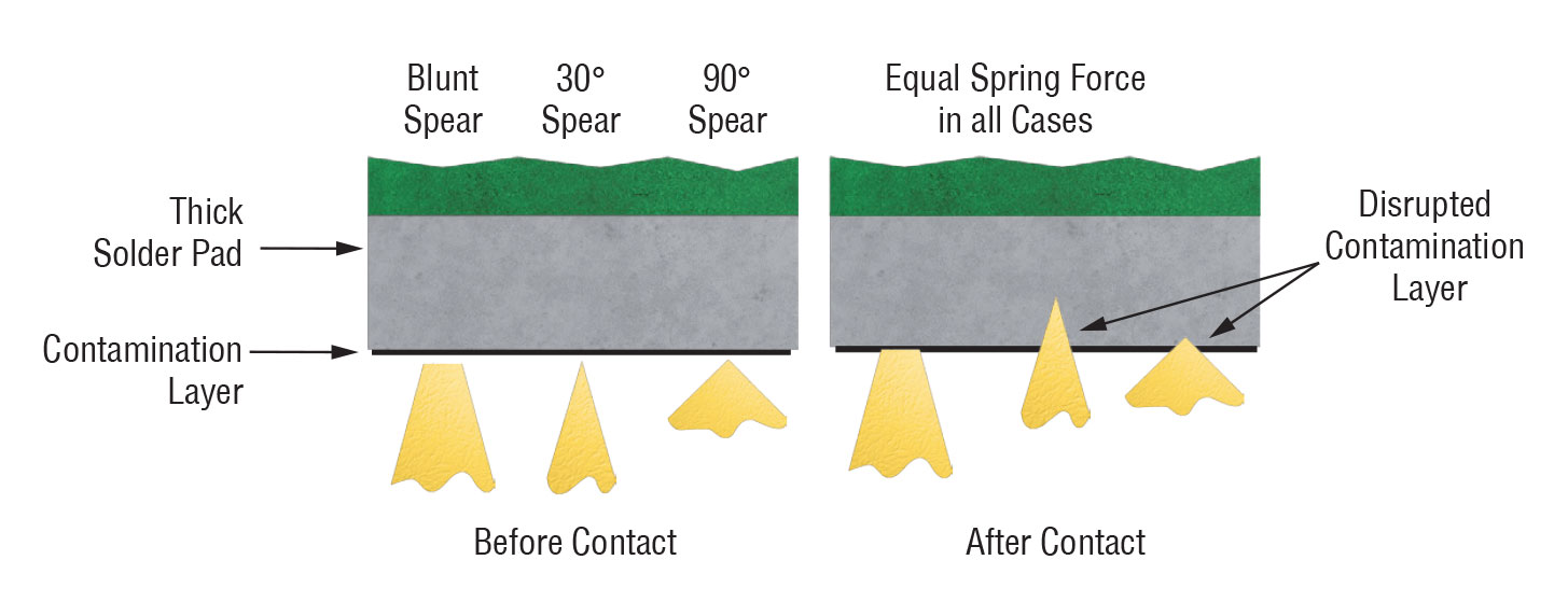
Geometry and sharpness will determine the ability to penetrate contamination layers. A tip that is blunt or has dull edges will make contact over a larger area thus reducing its ability to penetrate contamination layers on the test targets.
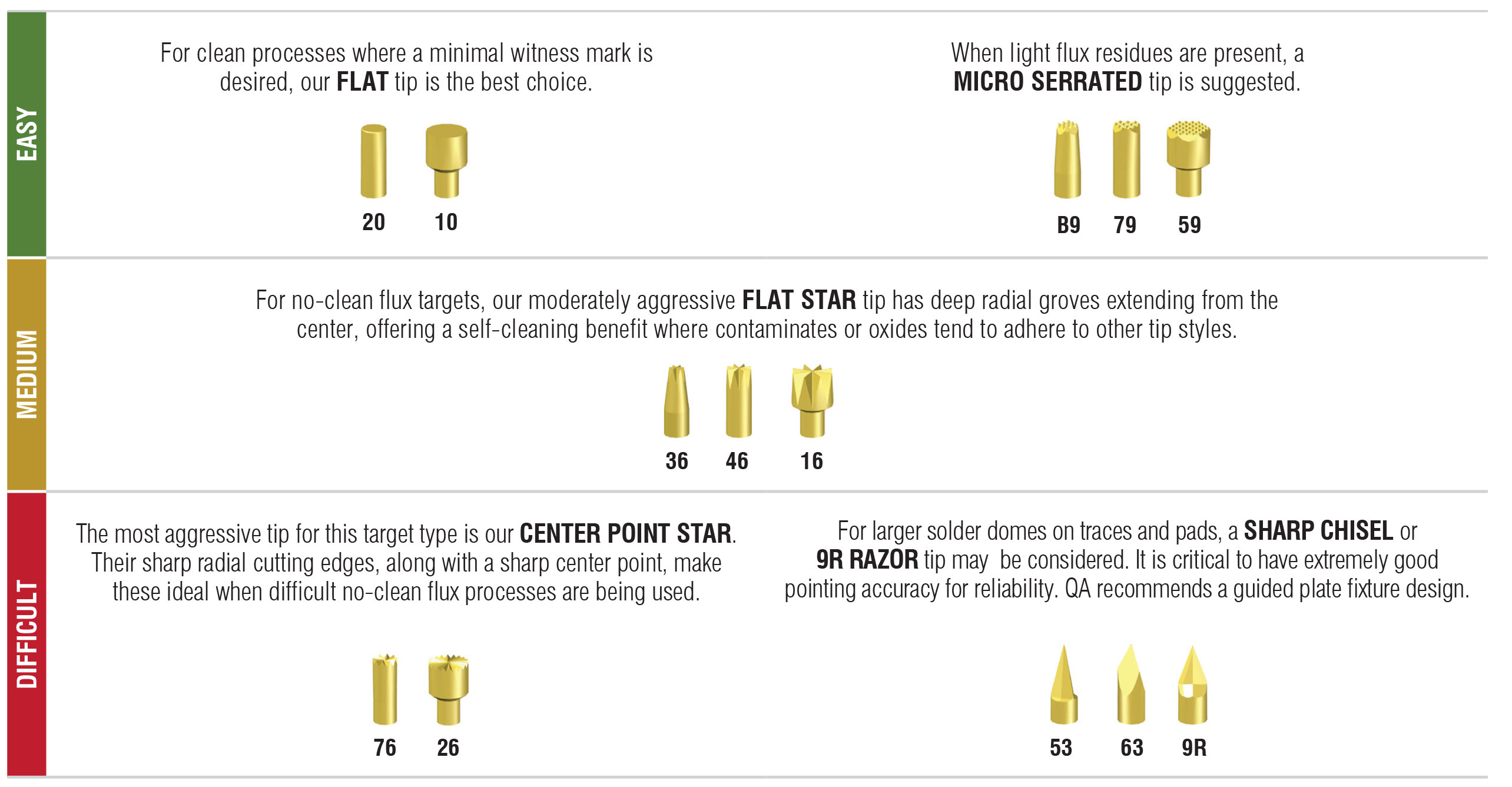
A tip that has a sharp point or steep cutting edges applies a higher pressure against the solder causing it to yield. As the solder yields, any oxides or remaining flux residues are disrupted, allowing better electrical contact.
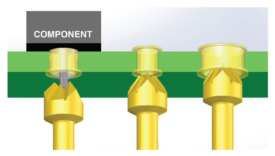
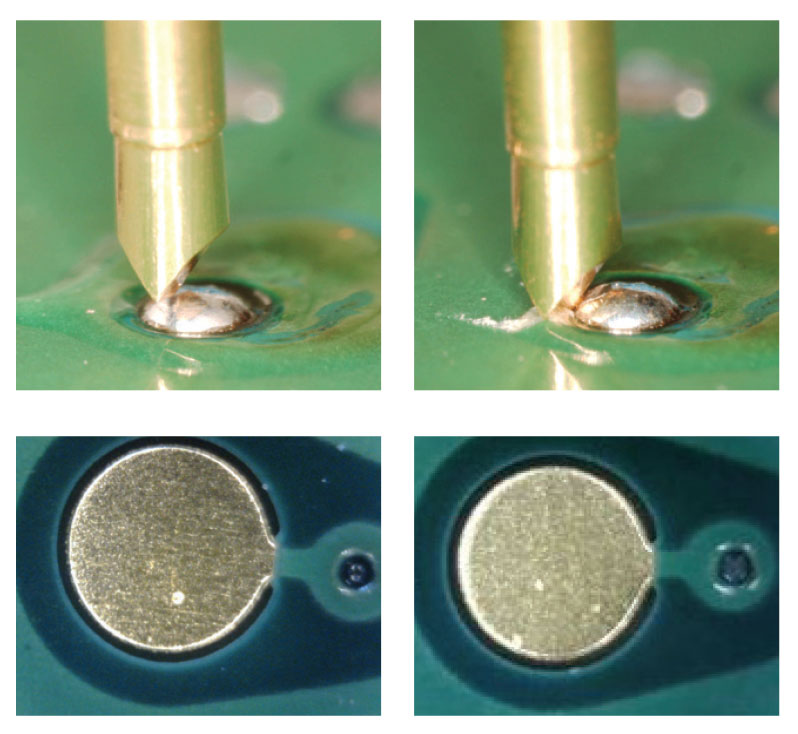
TEST PADS, VIAS and THROUGH-HOLES come in a wide range of sizes, surfaces, and shapes. They can be solder pasted, unpasted, concave, flat, or convex (dome).
Vias and through-holes in a PCB are typically used to pass a signal from one layer to another. When these are to be used as test points, it is necessary that they are not solder-masked so that they can be easily probed.

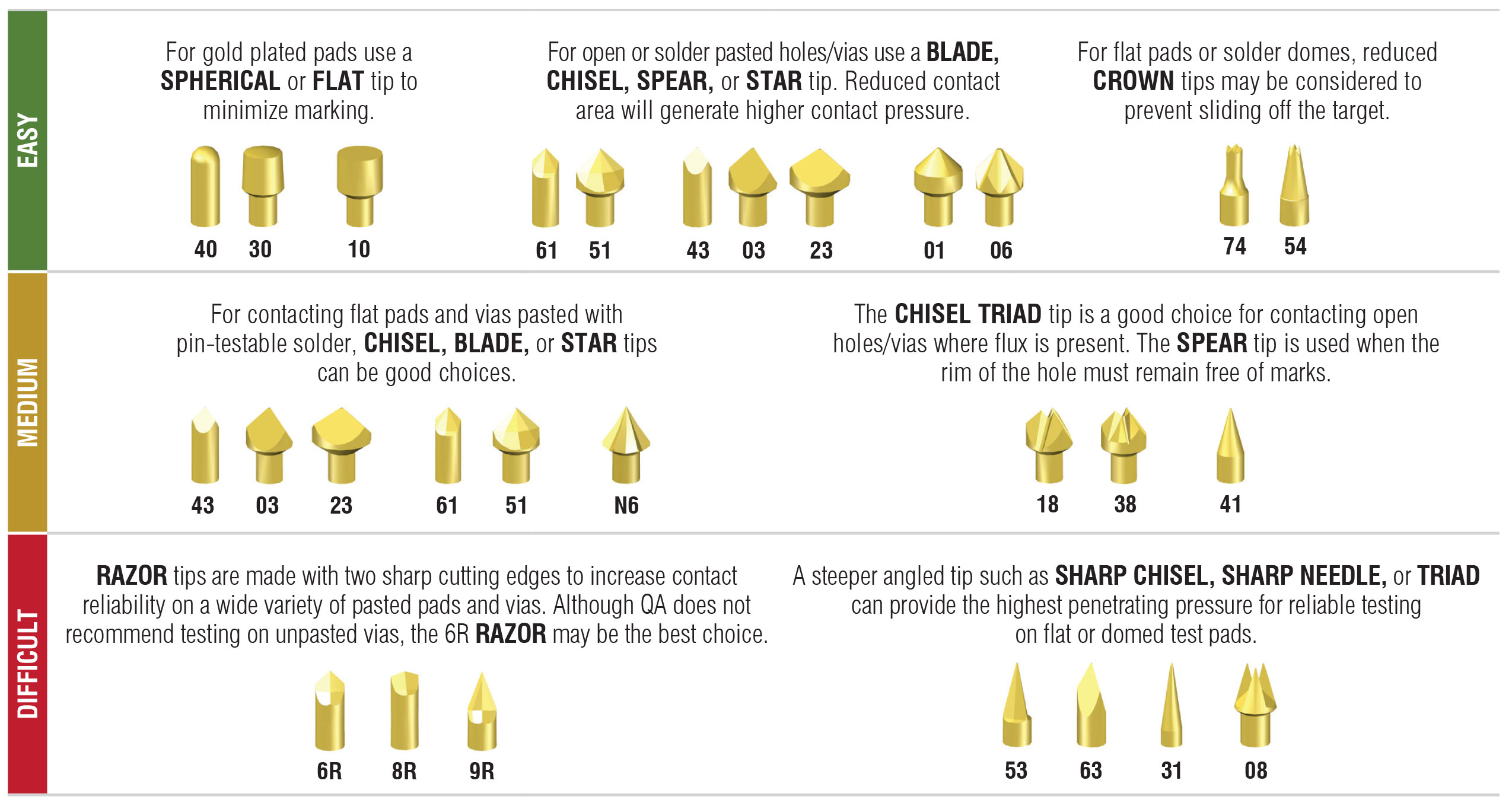
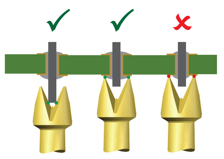
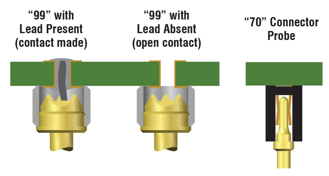
A lead is a terminal on a component. They could be different lengths, straight or bent. Smaller leads will require tip Styles with closely spaced cutting edges to trap the leads. A post is larger in diameter and more rigid than leads.
Multi-point tips are designed to capture a target, such as a lead or a post. Some styles have steeper valleys between the tips, creating a self-cleaning feature where it allows contamination to escape.

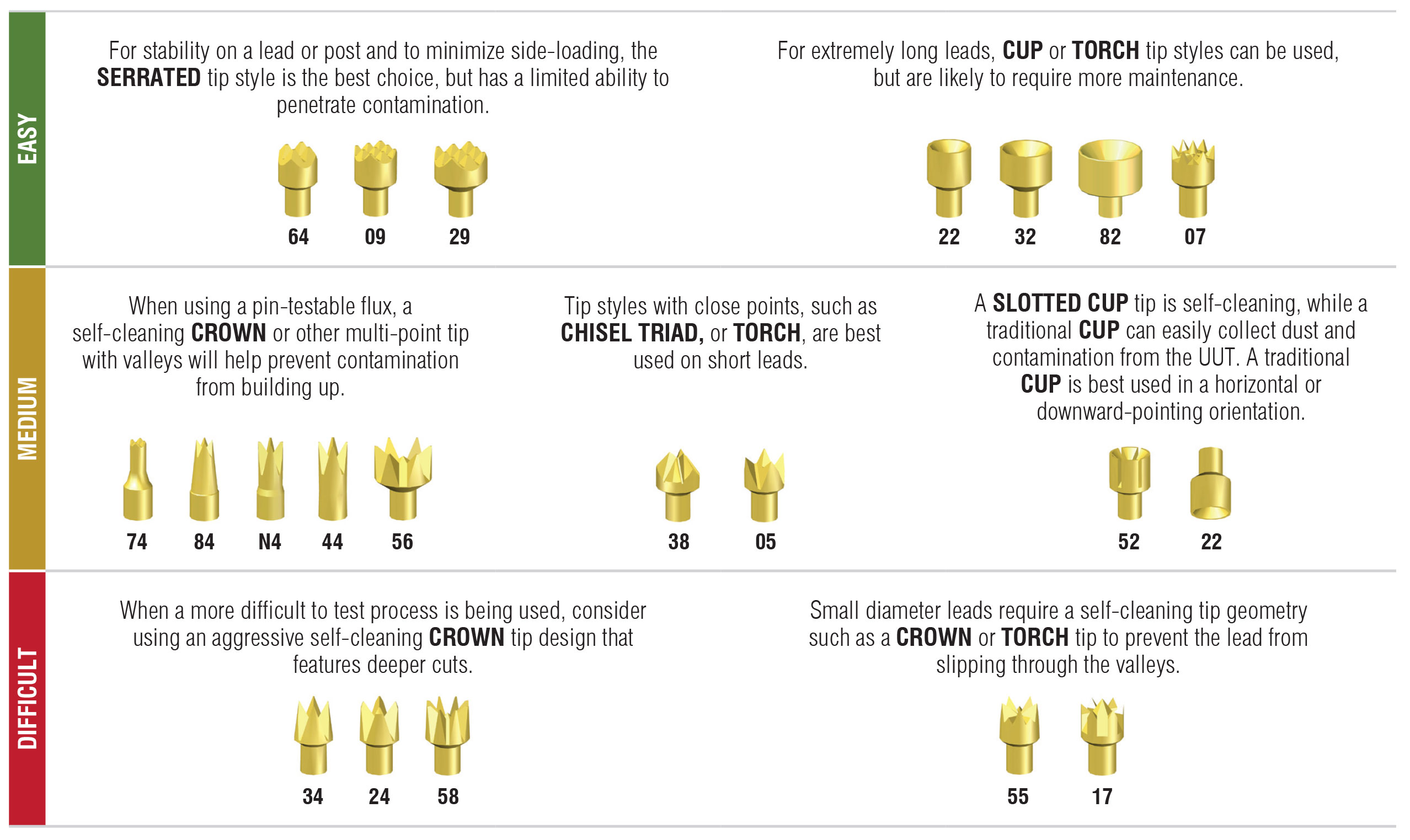
Technology provides test point accessibility, using a probe to contact a variety of solder beads or bumps that are placed on a trace where the solder mask has been removed. In addition, by placing an excessive amount of solder on vias or test pads, a round dome of solder may also need to be probed.

In addition, QA offers many specialty tip styles for other important, but less common applications.

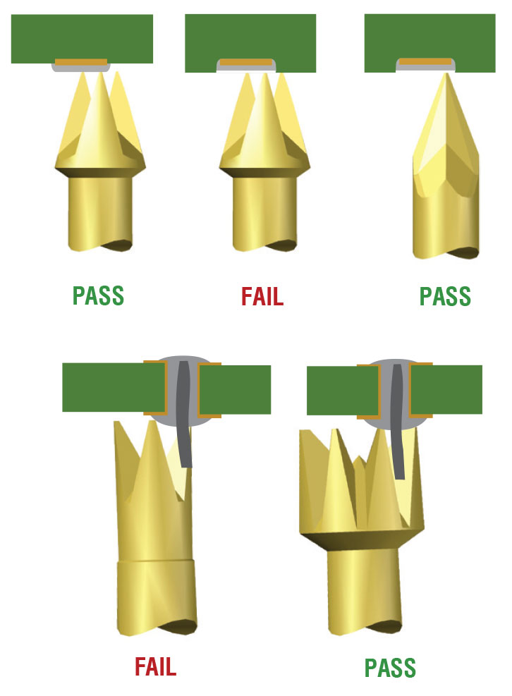
In summary, it is critical to select a tip style with the right number of points of contact, the correct angles, and sharpness. Improving the electrical contact to your test targets will help increase probe life and improve your FPY. Higher yields mean less time troubleshooting false failures, faster through-put, and ultimately, lower overall cost of test.